2024-12-11 08:22:00
spectrum.ieee.org
The semiconductor industry’s long held imperative—Moore’s Law, which dictates that transistor densities on a chip should double roughly every two years—is getting more and more difficult to maintain. The ability to shrink down transistors, and the interconnects between them, is hitting some basic physical limitations. In particular, when copper interconnects are scaled down, their resistivity skyrockets, which decreases how much information they can carry and increases their energy draw.
The industry has been looking for alternative interconnect materials to prolong the march of Moore’s Law a bit longer. Graphene is a very attractive option in many ways: The sheet-thin carbon material offers excellent electrical and thermal conductivity, and is stronger than diamond.
However, researchers have struggled to incorporate graphene into mainstream computing applications for two main reasons. First, depositing graphene requires high temperatures that are incompatible with traditional CMOS manufacturing. And second, the charge carrier density of undoped, macroscopic graphene sheets is relatively low.
Now, Destination 2D, a startup based in Milpitas, Calif., claims to have solved both of those problems. Destination 2D’s team has demonstrated a technique to deposit graphene interconnects onto chips at 300 °C, which is still cool enough to be done by traditional CMOS techniques. They have also developed a method of doping graphene sheets that offers current densities 100 times as dense as copper, according to Kaustav Banerjee, co-founder and CTO of Destination 2D.
“People have been trying to use graphene in various applications, but in the mainstream micro-electronics, which is essentially the CMOS technology, people have not been able to use this so far,” Banerjee says.
Destination 2D is not the only company pursuing graphene interconnects. TSMC and Samsung are also working to bring this technology up to snuff. However, Banerjee claims, Destination 2D is the only company to demonstrate graphene deposition directly on top of transistor chips, rather than growing the interconnects separately and attaching them to the chip after the fact.
Depositing graphene at low temperature
Graphene was first isolated in 2004, when researcher separated sheets of graphene by pulling them off graphite chunks with adhesive tape. The material was deemed so promising that in 2010 the feat garnered a Nobel prize. (Nobel Prize co-recipient Konstantin Novoselov is now Destination 2D’s chief scientist).
 Startup Destination 2D has developed a CMOS-compatible tool capable of depositing graphene interconnects at the wafer scale.Destination 2D
However, carefully pulling graphene off of pencil tips using tape is not exactly a scalable production method. To reliably create graphene structures, researchers have turned to chemical vapor deposition, where a carbon gas is deposited onto a heated substrate. This typically requires temperatures well above the roughly 400 °C maximum operating temperature in CMOS manufacturing.
Destination 2D uses a pressure-assisted direct deposition technique developed in Banerjee’s lab at the University of California, Santa Barbara. The technique, which Banerjee calls pressure-assisted solid phase diffusion, uses a sacrificial metal film such as nickel. The sacrificial film is placed on top of the transistor chip, and a source of carbon is deposited on top. Then, using a pressure of roughly 410 to 550 kilopascals (60 to 80 pounds per square inch), the carbon is forced through the sacrificial metal, and recombines into clean multilayer graphene underneath. The sacrificial metal is then simply removed, leaving the graphene on-chip for patterning. This technique works at 300 °C, cool enough to not damage the transistors underneath.
Boosting Graphene’s Current Density
After the graphene interconnects are patterned, the graphene layers are doped to reduce the resistivity and boost their current-carrying capacity. The Destination 2D team uses a doping technique called intercalation, where the doping atoms are diffused between graphene sheets.
The doping atoms can vary—examples include iron chloride, bromine, and lithium. Once implanted, the dopants donate electrons (or their in-material counterparts, electron holes) to the graphene sheets, allowing higher current densities. “Intercalation chemistry is a very old subject,” Banerjee says. “We are just bringing this intercalation into the graphene, and that is new.”
This technique has a promising feature—unlike copper, as the graphene interconnects are scaled down, their current-carrying capacity improves. This is because for thinner lines, the intercalation technique becomes more effective. This, Banerjee argues, will allow their technique to support many generations of semiconducting technology into the future.
Destination 2D has demonstrated their graphene interconnect technique at the chip level, and they’ve also developed tools for wafer-scale deposition that can be implemented in fabrication facilities. They hope to work with foundries to implement their technology for research and development, and eventually, production.
From Your Site Articles
Related Articles Around the Web
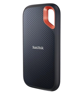
Keep your files stored safely and securely with the SanDisk 2TB Extreme Portable SSD. With over 69,505 ratings and an impressive 4.6 out of 5 stars, this product has been purchased over 8K+ times in the past month. At only $129.99, this Amazon’s Choice product is a must-have for secure file storage.
Help keep private content private with the included password protection featuring 256-bit AES hardware encryption. Order now for just $129.99 on Amazon!
Support Techcratic
If you find value in Techcratic’s insights and articles, consider supporting us with Bitcoin. Your support helps me, as a solo operator, continue delivering high-quality content while managing all the technical aspects, from server maintenance to blog writing, future updates, and improvements. Support Innovation! Thank you.
Bitcoin Address:
bc1qlszw7elx2qahjwvaryh0tkgg8y68enw30gpvge
Please verify this address before sending funds.
Bitcoin QR Code
Simply scan the QR code below to support Techcratic.

Please read the Privacy and Security Disclaimer on how Techcratic handles your support.
Disclaimer: As an Amazon Associate, Techcratic may earn from qualifying purchases.


